A Simplified Power Supply Design Using the Tl494 Control Circuit

The IC TL494 is a versatile PWM control IC, which can be applied in many different ways in electronic circuits. In this articles we discuss in detail regarding the main functions of the IC, and also how to use it in practical circuits.
General Description
The IC TL494 is specifically designed for single chip pulse width modulation application circuits. The device is mainly created for power supply control circuits, which can be efficiently dimensioned using this IC.
The device comes with an in-built variable oscillator, a dead-time controller stage (DTC), a flip flop control for pulse-steering, a precision 5 V regulator, two error amps, and some output buffer circuits.
The error amplifiers feature a common mode voltage range from - 0.3 V to VCC - 2V.
The dead time control comparator is set with a fixed offset value for delivering a constant 5% dead time approximately.
The on chip oscillator function can be overridden by connecting the RT pin#14 of the IC with reference pin#14, and by externally providing a sawtooth signal to the CT pin#5. This facility also allows driving many TL494 ICs synchronously having different power supply rails.
The output transistors inside the chip having floating outputs are arranged to deliver either a common-emitter output or a emitter-follower output facility.
The device allows the user to get either a push-pull type or a single ended oscillation across its output pins by appropriately configuring pin#13, which is the output-control function pin.
The internal circuitry makes it impossible for any of the outputs to produce a double pulse, while the IC is wired in the push-pull function.
Pin Function and Configuration
The following diagram and explanation provide us the basic information regarding the pin function for the IC TL494.
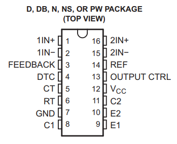
- Pin#1 and Pin#2 (1 IN+ and 1IN-) : These are the non-inverting and inverting inputs of the error amplifier (op amp 1).
- Pin#16, Pin#15 (1 IN+ and 1IN-) : As above these are the non-inverting and inverting inputs of the error amplifier (op amp 2).
- Pin#8 and Pin#11 (C1, C2): These are the outputs 1 and 2 of the IC which connect with the collectors of the respective internal transistors.
- Pin#5 (CT): This pin needs to be connected with an external capacitor for setting the oscillator frequency.
- Pin#6 (RT): This pin needs to be connected with an external resistor for setting the oscillator frequency.
- Pin#4 (DTC): It's the input of the internal op amp which controls the dead-time operation of the IC.
- Pin#9 and Pin#10 (E1 and E2): These are the outputs of the IC which connect with emitter pins of the internal transistor.
- Pin#3 (Feedback): As the name suggests, this input pin is used for integrating with an output sample signal for a desired automatic control of the system.
- Pin#7 (Ground): This pin is the ground pin of the IC, which needs to connected with the 0 V of the supply source.
- Pin#12 (VCC): This is the positive supply pin of the IC.
- Pin#13 (O/P CNTRL): This pin can be configured for enabling the output of the IC in the push-pull mode or single ended mode.
- Pin#14 (REF): This output pin provides a constant 5V output which can be used for fixing a reference voltage for the error op amps, in the comparator mode.
Absolute Maximum Ratings
- (VCC) Maximum Supply voltage not to exceed = 41 V
- (VI) Maximum Voltage on input pins not to exceed = VCC + 0.3 V
- (VO) Maximum output voltage at collector of internal transistor = 41 V
- (IO) Maximum current on Collector of the internal transistor = 250 mA
- Maximum IC pin soldering heat at 1.6 mm (1/16 inch) away from IC body not to exceed 10 seconds @ 260 °C
- Tstg Storage temperature range = –65/150 °C
Recommended Operating Conditions
The following data gives you the recommended voltages and currents that can be used for operating the IC under safe and efficient conditions:
- VCC supply: 7 V to 40 V
- VI Amplifier Input Voltage: -0.3 V to VCC - 2 V
- VO Transistor Collector Voltage = 40, Collector Current for each Transistor = 200 mA
- Current into Feedback pin: 0.3 mA
- fOSC Oscillator frequency range: 1 kHz to 300 kHz
- CT Oscillator timing capacitor value: Between 0.47 nF to 10000 nF
- RT Oscillator timing resistor value: Between 1.8 k to 500 k Ohms.
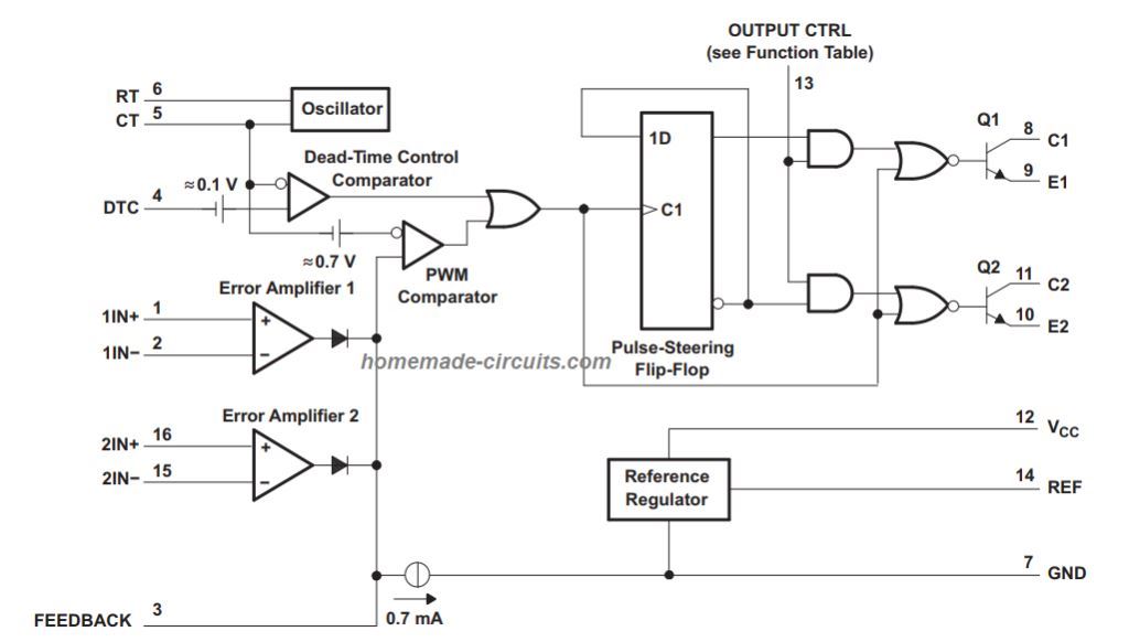
Internal Layout Diagram
How to Use IC TL494
In the following paragraphs we learn the important functions of the IC TL494, and how to use it in PWM circuits.
Overview: The TL494 IC is designed in such a way that it not only features the important circuitry needed to control a switching power supply, but additionally tackles several fundamental difficulties and minimizes the need of supplemental circuit stages necessary in the overall structure.
The TL494 is basically a fixed-frequency pulse-width-modulation (PWM) control circuit.
The modulation function of output pulses is achieved when the internal oscillator compares its sawtooth waveform through the timing capacitor (CT) with both pairs of control signals.
The output stage is toggled in the period when the sawtooth voltage is higher than the voltage control signals.
As the control signal increases, the time when the sawtooth input is higher decreases; consequently, the output pulse length reduces.
A pulse-steering flip-flop alternately guides the modulated pulse to each of the two output transistors.
5-V Reference Regulator
The TL494 creates a 5 V internal reference which is fed to the REF pin.
This internal reference helps to develop a stable constant reference, which acts like a pre-regulator for ensuring a stable supply. This reference is then reliably used for powering various internal stages of the IC such as logic output control, flip flop pulse steering, oscillator, dead time control comparator, and PWM comparator.
Oscillator
The oscillator generates a positive sawtooth waveform for the dead-time and the PWM comparators so that these stages can analyze the various control input signals.
It's the RT and the CT which are responsible for determining the oscillator frequency and thus can be externally programmed.
The sawtooth waveform generated by the oscillator charges the external timing capacitor CT with a constant current, determined by the complementing resistor RT.
This results in the creation of a linear-ramp voltage waveform. Each time the voltage across CT reaches 3 V, the oscillator quickly discharges it, which subsequently restarts the charging cycle. The current for this charging cycle is calculated through the formula:
Icharge = 3 V / RT --------------- (1)
The period of the sawtooth waveform is given by:
T = 3 V x CT / Icharge ----------(2)
The oscillator frequency is thus determined using the formula:
f OSC = 1 / RT x CT ---------------(3)
However, this oscillator frequency will be compatible with the output frequency when the output is configured as single-ended. When configured in push-pull mode, the output frequency will be 1/2 of the oscillator frequency.
Therefore, for single ended output the above equation no 3 can be used.
For push pull application the formula will be:
f = 1 / 2RT x CT ------------------(4)
Dead-time Control
The dead-time pin set-up regulates the minimum dead time (off periods between the two outputs).
In this function when voltage on the DTC pin exceeds the ramp voltage from the oscillator, forces the output comparator to switch OFF the transistors Q1 and Q2.
The IC has an internally set offset level of 110 mV that guarantees a minimum dead time of around 3% when the DTC pin is connected with the ground line.
The dead time response can be increased by applying an external voltage to the DTC pin#4. This allows to have a linear control over the dead-time function from the default 3% to a maximum of 100%, through a variable input of 0 to 3.3 V.
If a full range control is used, the output can of the IC can be regulated through an external voltage without disturbing the error amplifier configurations.
The dead-time feature can be employed in situations where added control of the output duty cycle becomes necessary.
But for proper functioning it must be ensured that this input is either terminated to a voltage level or to ground and should be never left floating.
Error Amplifiers
The two error amplifiers of the IC have a high gain, and are biased through the ICs VI supply rail. This enables a common-mode range of input from -0.3 V to VI - 2 V.
Both the error amplifiers are internally set up to work like a single-ended single supply amplifiers, wherein each output have active-high capability only. Due to this capability, the amplifiers are able to activate independently for satisfying a narrowing PWM demand.
Since the outputs of the two error amps are tied like OR gates with the input node of the PWM comparator, the amplifier which can work with minimum pulse out dominates.
The amplifiers have their outputs biased with a low current sink so that the the IC output ensures maximum PWM when the error amplifiers are in the non-functional mode.
Output-Control Input
This pin of the IC can be configured to allow the IC output to either work in a single ended mode that is both output oscillating together in parallel or in push pull manner producing alternately oscillating outputs.
The output-control pin works asynchronously, enabling it to have a direct control over the output of the IC, without affecting the internal oscillator stage or the flip flop pulse-steering stage.
This pin is normally configured with a fixed parameter as per the application specifications. For example, if the IC outputs are intended to work in parallel or single ended manner, the output-control pin is connected with the ground line permanently. Due to this the pulse-steering stage inside the IC gets disabled and the alternate flip flop stops at the output pins.
Also, in this mode the pulses arriving at the dead-time control and PWM comparator are carried together by both the output transistors, allowing the output to switch ON/OFF in parallel.
For obtaining a push pull output operation, the output-control pin simply needs to be connected to the +5V output reference pin (REF) of the IC. In this condition, each of the output transistors turn ON alternately through the pulse-steering flip-flop stage.
Output Transistors
As can be seen the second diagram from top, the chip consists of two output transistors, which having uncommitted emitter and collector terminals.
Both these floating terminals are rated to sink (take in) or source (give out) up to 200 mA current.
The saturation point of the transistors is less than 1.3 V when configured in the common-emitter mode, and less than 2.5 V in the common-collector mode.
They are internally protected from short circuit and over current.
Application Circuits
As explained in the above, the TL494 is primarily a PWM controller IC, therefore the main application circuits are mostly PWM based circuits.
A couple of example circuits are discussed below, which can be modified in various ways as per individual requirements.
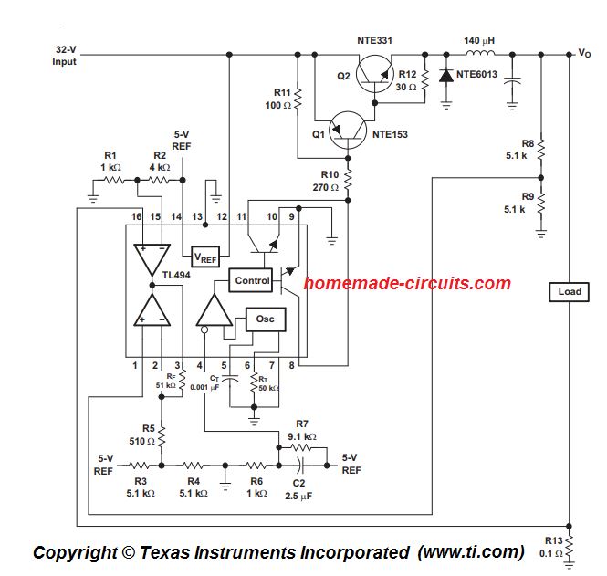
Solar Charger using TL494
The following design shows how the TL494 can be effectively configured to create a 5-V/10-A switching buck power supply.
In this configuration the output works in parallel mode, and therefore we can see the output-control pin#13 is connected to ground.
The two error amps are also used very efficiently here. One error amplifier controls the voltage feedback via R8/R9 and keep the output constant at the desired rate (5V)
The second error amplifier is used for controlling the maximum current via R13.
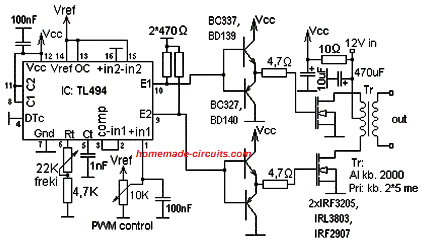
TL494 inverter
Here's a classic inverter circuit built around the IC TL494. In this example the output is configured to work in the push-pull manner, and therefore the output-control pin here is connected with the +5V reference, which is achieved from pin#14. The erst of the pins are also configured exactly as described in the above datasheet.
Conclusion
The IC TL494 is a PWM control IC with highly accurate output and feedback control facilities ensuring an ideal pulse control for any desired PWM circuit application.
It is similar to SG3525 in many ways, and can be used as an effective replacement for it, although the pin numbers can be different and not exactly compatible.
If you have any questions pertaining to this IC, please feel free to ask them through the comments below, I'll be happy to help!
Reference: TL494 datasheet
A Simplified Power Supply Design Using the Tl494 Control Circuit
Source: https://www.homemade-circuits.com/tl494-datasheet-pinout-application-circuits/
0 Response to "A Simplified Power Supply Design Using the Tl494 Control Circuit"
Post a Comment